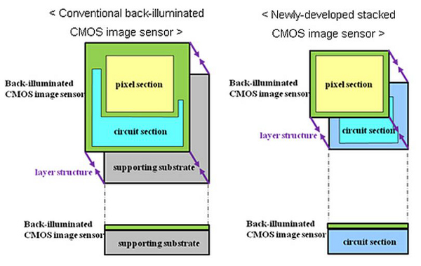
Sony Corporation on Monday announced that it is working on a new design for CMOS image sensors that will be used in camera modules for smartphones, tablets, and other mobile applications. This model of sensor includes built-in signal processing functionality, a task which used to be handled by external elements, and that it can handle advanced imaging tasks in an even smaller profile.
The design is what is known as a stacked CMOS sensor, and Sony has turned two major elements of the sensor into independent components. The stack puts the "pixel section" and "circuit section" fully on top of one another rather than fitting them on the same board side-by-side.
Sony says it has devised models of this sensor that utilize "RGBW Coding" for lower noise images in low light conditions, and "HDR (High Dynamic Range) Movie" functionality for improving color in flooded light situations.
With cutting-edge smartphones and tablets donning multiple cameras, and advancements taking place in camera-based, Kinect-style interfaces, the image sensor business is booming. In late 2010, Sony committed to taking charge of the market, and purchased a Nagasaki semiconductor facility from Toshiba to effectively double its capacity for CMOS sensor production to around 40,000 units per month.
However, the natural disasters that hit Japan in 2011 had a serious impact on all Japanese imaging companies, and they are believed to have caused a delay in Sony's development of these very sensors.
These sensors won't sample to manufacturers until March 2012, putting Sony a few months behind Samsung, which unveiled its new smartphone camera modules last September.
Samsung's units are capable of 16 megapixel stills and native 16:9 video at up to 8.3 megapixel resolution at 60 frames per second. Samsung also debuted its forward-facing camera unit at the same time: a 1.2-Megapixel (Mp), 1/8.2-inch CMOS image sensor system-on-chip that can fit into a 5.5 x 5.5mm camera module with profile of only 2.8mm.

